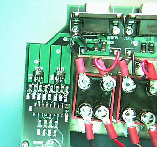
These little guys were designed to be get pretty hot in normal operation but since they don't have a lot of surface area to disipate the heat, the manufacturer recommended putting in very large pads (anchor points for the chips) to act as heat sinks. The four lighter green areas in this photo are those heat sink and pad combinationss. You'll also notice that the lines leading away from these large pads are very thick, so they can handle the large currents running through the FETs without burning up or melting.
The large black component just below the FETs, is called an opto-isolater. It uses light to transmit signals so that 2 circuits can communicate with each other, but remain electrically isolated. In this case, I am isolating the high current FETs (above the opto-isolator) from the rest of the circuitry (below the opto-isolator), wich uses lower currents and voltages.